|
| Our Equipment | General Description | | |
|---|
| FEI Helios NanoLab™ 600 | 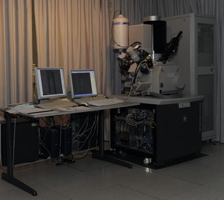 | What puts the Helios NanoLab in a class of its own is its ability to offer the highest imaging, contrast, stability and speed performance together with the largest range of SEM / FIB applications. It ensures best resolution, reproducible metrology and best control of the beam for writing purposes. The outstanding imaging capabilities of the Helios NanoLab start with its novel FESEM tec...
|
More info for students
|
More info for companies
| | Transmission electron Microscope | .jpg) | FEI CM 120 EDS Edax DX-4
120kV, analytical with LaB6 filament, sample holder with 5 axes motorized. Linear resolution of 0.2nm. EDS probe with range of detectable elements since borum, resolution MnKa 134eV, digital acquisition of rX compositional profile and maps.Software for quantitative-semiquantitative analysis using ZAF and PhiRhoZ models.TEM CCD: Effecti...
|
More info for students
|
More info for companies
| | Bruker D8 Discover DaVinci Xray Diffractometer | 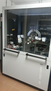 | The D8 Discover is an all purpose X-ray analyzer which can be configured for a great range of diffraction applications: powder diffraction, including phase identification and quantitative phase analysis, micro-structure and crystal structure analysis, film analysis, residual stress and texture investigations. This device can therefore be used for many purposes, such as studying the crystal struct...
|
More info for students
|
More info for companies
| | Agilent NANO Indenter® G200 | 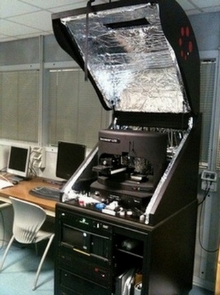 | Nano Indenter G200 system represents the market’s most advanced platform for exploring small-scale material behavior. In addition to incorporating the latest technologies for sample positioning, data acquisition and control conforms to ISO 14577-1, 2 & 3. Through its design and the control it affords you as the user, the Nano Indenter G200 system provides a fast and reliable way to acqui...
|
More info for students
|
More info for companies
| | Scanning electron Microscope | 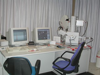 | SEM stands for scanning electron microscope. The SEM is a microscope that uses electrons instead of light to form an image. The scanning electron microscope has many advantages over traditional microscopes. The SEM has a large depth of field, which allows more of a specimen to be in focus at one time. The SEM also has much higher resolution, so closely spaced specimens can be magnified at much...
|
More info for students
|
More info for companies
|
1
- 5  |
|
|
|
|
| Pub Year | Title | Authors | Published in
|
|---|
| 2017 | Atomic Layer Deposition of Semiconductor Oxides on Electric Sail Tethers | Mehwish Hassan, PhD; Laura Borgese, PhD; Giuditta Montesanti; Edoardo Bemporad, Prof.; Gianmario Cesarini; Roberto Li Voti; Laura E Depero, Prof. | Thin Solid Films | | | 2016 | Effect of lithiation on micro-scale fracture toughness of LixMn2O4 cathode | M. Z. Mughal, R. Moscatelli, H-Y Amanieu, M. Sebastiani | Scripta Materialia | | | 2016 | Low temperature degradation resistant nanostructured yttria-stabilized zirconia for dental applications | I.G. tredici, M. Sebastiani, F. Massimi, E. Bemporad, A. Resmini, G. Merlati, U. Anselmi-Tamburini | Ceramics International | | | 2016 | High-resolution high-speed nanoindentation mapping of cement pastes: unravelling the effect of microstructure on the mechanical properties of hydrated phases | M. Sebastiani, R. Moscatelli, F. Ridi, P. Baglioni F. Carassiti | Materials & Design | | | 2016 | An Improved Instrument and Methodology for Complex Micro-scale Abrasion Tests | Montesanti G; Di Cesare C; Bemporad E | NOT YET PUBLISHED | | | 2016 | Experimental and modelling characterisation of residual stresses in cylindrical samples of rapidly cooled bulk metallic glass | A. M. Korsunsky, T. Sui, E. Salvati, E. P. George, M. Sebastiani | Materials and Design | | | 2016 | Load displacement and high speed nanoindentation data set at different state of charge (SoC) for spinel LixMn2O4 cathodes | M. Z. Mughal, R. Moscatelli, M. Sebastiani | Data in Brief | | | 2016 | Determination of the elastic moduli and residual stresses of freestanding Au-TiW bilayer thin films by nanoindentation | M. Ghidelli, M. Sebastiani, Christian Collet, Raphael Guillemet | Materials and Design | | | 2016 | Nanotechnology the key to growth in Europe | - | Platinum ( Research & Innovation) | | | 2016 | Design, fabrication and characterisation of multilayer Cr-CrN thin coatings with tailored residual stress profiles | M. Renzelli, M. Z. Mughal, M. Sebastiani, E. Bemporad | Materials and Design | | | 2016 | Effect of elastic anisotropy on strain relief and residual stress determination in cubic systems by FIB-DIC experiments | M. Krottenthaler, L. Benker, M.Z. Mughal, M. Sebastiani, K. Durst, M. Göken | Materials and Design | | | 2015 | A novel pillar indentation splitting test for measuring fracture toughness of thin ceramic coatings | M. SEBASTIANI, K. E. Johanns, E. G. Herbert, F. Carassiti, G. M. Pharr | Philosophical Magazine | | | 2015 | Multi-scale Assessment of the Toughness of a PVD Coating | Renzelli M, Bemporad E | Proceedings of the 28th International Conference on Surface Modification Technologies 28 (SMT-28) | | | 2015 | Role of grain boundaries and micro-defects on the mechanical response of a crystalline rock at multiscale | Bandini, A., Berry P., Bemporad E., Sebastiani M., Chicot D. | International Journal of Rock Mechanics and Mining Sciences | | | 2015 | Structural, morphological and mechanical characterization of Mo sputtered coatings | Deambrosis M. S., Miorin E., Montargen F., Zin V., Fabrizio M., Sebastiani M., Massimi F., Bemporad E. | Surface and Coatings Technology | |
| 1
- 15 |
|
|
|